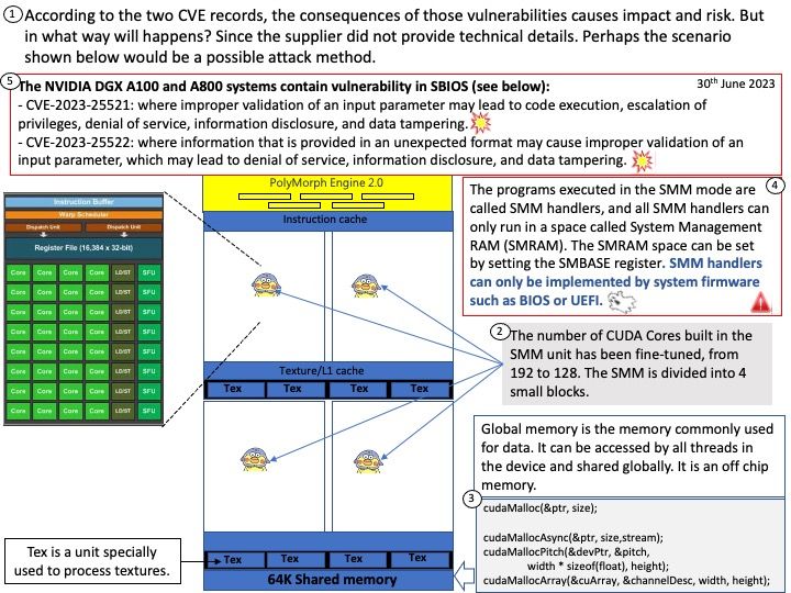
Preface: The A800 has a data transfer rate of 400GB/s and the A100 is 600GB/s, and as such complies with the 600GB/s or less.
Background: What is SMM? It turned out to be SM in the Fermi era and SMX in the Kepler era. If you enlarge the SMX core of Kepler, you will see more LD/ST access units than Fermi, which also means that
the number of execution threads processed by Kepler in a single cycle is higher than that of Fermi.
Streaming Multiprocessor composed of CUDA Core, PolyMorph Engine and other units.
Simply put, it is to fine-tune the number of CUDA Cores built in the SMM unit from 192 to 128. The SMM is divided into 4 small blocks,
and each block has an independent control logic (Control Logic). In the past, these control logics needed to be responsible for a large number of CUDA Cores. Through small blocks.
Vulnerability details:
CVE‑2023‑25521: The NVIDIA DGX A100 and A800 systems contain a vulnerability in SBIOS, where improper validation of an input parameter
may lead to code execution, escalation of privileges, denial of service, information disclosure, and data tampering.
CVE-2023-25522: The NVIDIA DGX A100 and A800 systems contain a vulnerability in SBIOS, where information that is provided
in an unexpected format may cause improper validation of an input parameter, which may lead to denial of service, information disclosure, and data tampering.
Best practice: Disable all features in the UEFI and OS, that are not used. This reduces the attack surface.
Configure your system to only execute signed code and signed kernel modules, if possible.
Official announcement: For details, please refer to link – https://nvidia.custhelp.com/app/answers/detail/a_id/5461